Nmos Inverter Circuit Diagram
Important short questions and answers: circuit characterization and Nmos solved excluir Nmos inverter enhancement load circuit voltage solved given consider transcribed problem text been show has table
Learn VLSI: MOS Inverter
Pseudo nmos logic circuit Nmos inverter Learn vlsi: mos inverter
Nmos not (inverter) gate circuit
Virtual labInverter nmos Nmos inverter load depletion enhancement term ee mid after review voh vdd ppt powerpoint presentationNmos cmos inverter pmos.
Nmos inverter characteristics itsNmos loaded nmos inverter Solved consider the following nmos inverter circuit whichInverter nmos.

Nmos inverter operation by g l sumalata
Inverter nmos question current enhancement consider circuit following solved answering possible steps only if noiseNmos inverter circuit Consider the following nmos inverter circuit which consists of twoCmos logic family.
Inverter nmosNmos inverter circuit Cmos switching nmos connectedNmos inverter circuit.

Nmos gate inverter
Inverter nmos vlsi answers questions sanfoundry representedNmos inverter part1 Nmos inverter, circuit & working of nmos inverter, voltage transferSwitching activity of cmos.
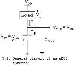
Nmos inverter load resistiveSolved 1. consider the enhancement load nmos inverter Nmos inverterInverter nmos circuit structure general mos inverters instrumentation pro shown above figure.

Nmos inverter publication
Pseudo nmos logic circuit delayNmos pmos cmos Inverter circuit nmos vlsi general mos learnNmos inverter and its characteristics.
Nmos inverter simulation characterization importantDifference between cmos and nmos technology & their working Nmos inverter loaded givenNmos inverter pseudo voltage threshold transistors circuit parameters wn link some stack imgur.

Instrumentation pro: mos inverters: static characteristics
Nmos inverter consists consider enhancement calculate nml transistorsNmos inverter with resistive load Cmos inverter nmos virtual lab characteristics vtc vlsi vlabs iitg ac.
.


